Embark on a journey with the comet project: on the trail of new semiconductor chips, a deep dive into the fascinating world of cutting-edge technology. This exploration delves into the ambitious goals and scope of the project, aiming to revolutionize the semiconductor industry. We’ll uncover the key challenges, innovative design methodologies, and groundbreaking materials that are shaping the future of computing.
The semiconductor landscape is constantly evolving, with established giants and emerging trends vying for dominance. We’ll examine the current state of the industry, from the dominant players to the latest advancements in chip design and manufacturing. The Comet Project is at the forefront, pushing boundaries and exploring novel approaches to create faster, more efficient, and more powerful chips.
Overview of the Comet Project
The Comet Project, a collaborative endeavor, focuses on advancing semiconductor chip technology. Its primary aim is to accelerate the development of next-generation chips, improving performance and efficiency while addressing critical industry challenges. This project has a specific scope, including geographical reach and industry focus.
Goals of the Comet Project
The Comet Project’s central goal is to significantly enhance the capabilities of semiconductor chips. This involves several key objectives:* Boosting processing speeds to handle complex calculations more efficiently.
- Reducing power consumption, leading to more energy-efficient devices.
- Miniaturizing chip components to increase the density of transistors.
- Improving the reliability and lifespan of chips.
- Reducing manufacturing costs to make advanced chips more accessible.
Scope of the Comet Project
The project has a broad scope, encompassing several aspects of semiconductor development.* Geographical Reach: The Comet Project operates globally, with collaborative partnerships across multiple countries. This international approach allows for the sharing of expertise and resources.
Industry Focus
The project targets various industries heavily reliant on advanced chips, including:
Artificial Intelligence (AI)
Developing chips optimized for AI algorithms.
High-Performance Computing (HPC)
Creating chips for supercomputers and data centers.
Consumer Electronics
Designing chips for smartphones, laptops, and other devices.
Automotive
Producing chips for autonomous driving and vehicle control systems.
Technological Focus
The project concentrates on several key technological areas:
Advanced Materials
Researching and implementing new materials with superior electrical properties.
New Architectures
Exploring innovative chip designs beyond traditional architectures.
Manufacturing Processes
Developing advanced manufacturing techniques for higher precision and efficiency.
Key Challenges the Comet Project Aims to Overcome
The Comet Project tackles several significant challenges in the semiconductor industry.* Moore’s Law Limitations: The project seeks to overcome the slowing pace of Moore’s Law, which states that the number of transistors on a microchip doubles approximately every two years. This is achieved by exploring alternative chip designs and manufacturing processes.
Example
* Intel’s development of 3D transistors (FinFET) represents a step towards overcoming Moore’s Law limitations by allowing for more transistors in a smaller space.
Power Consumption
Reducing power consumption is a major challenge. The project aims to create chips that are both powerful and energy-efficient.
Example
* The development of low-power processors for mobile devices, such as ARM-based chips, demonstrates the focus on energy efficiency.
Heat Dissipation
As chips become more powerful, managing heat becomes increasingly difficult. The project explores advanced cooling solutions and materials to mitigate this issue.
Example
* The use of liquid cooling systems in high-performance computers is a response to the challenge of heat dissipation.
Manufacturing Complexity
The manufacturing process for advanced chips is extremely complex and expensive. The project aims to develop more efficient and cost-effective manufacturing techniques.
Example
* The adoption of EUV (Extreme Ultraviolet) lithography represents a significant advancement in chip manufacturing, allowing for the creation of smaller and more complex chip features.
Material Science Limitations
Finding new materials that can replace silicon and perform better is a significant challenge. The project investigates materials like graphene and other 2D materials to improve chip performance.
Example
* Research into the use of gallium nitride (GaN) in power electronics is an example of exploring new materials for improved efficiency and performance.
The Semiconductor Chip Landscape
The semiconductor industry is a dynamic and critical sector, underpinning nearly every aspect of modern technology. From smartphones and computers to cars and industrial equipment, chips are the brains of our digital world. Understanding the current state and emerging trends within this landscape is crucial for anyone interested in the future of technology.
Dominant Players and Market Share
The semiconductor market is highly concentrated, with a few key players controlling a significant portion of the global market share. This dominance has a profound impact on innovation, pricing, and the overall supply chain.
| Company | Approximate Market Share (2023) | Key Products |
|---|---|---|
| Intel | 15% | CPUs, GPUs, Chipsets |
| Samsung | 11% | Memory chips (DRAM, NAND), Processors, Foundry Services |
| TSMC (Taiwan Semiconductor Manufacturing Company) | 57% (Foundry Market) | Foundry Services (manufacturing chips for various companies) |
| Qualcomm | 5% | Mobile processors (Snapdragon), Modems |
| Broadcom | 3% | Networking chips, Wireless connectivity chips |
Note: Market share percentages are approximate and can vary depending on the source and specific market segment considered. TSMC’s market share refers specifically to the foundry market, where it manufactures chips for other companies.
Emerging Trends in Chip Design and Manufacturing
The semiconductor industry is constantly evolving, driven by the relentless pursuit of increased performance, reduced power consumption, and smaller form factors. Several key trends are reshaping chip design and manufacturing processes.
- Advanced Materials: Traditional silicon is reaching its physical limits. Researchers are exploring new materials like gallium nitride (GaN) and silicon carbide (SiC) for power electronics, offering higher efficiency and improved performance at elevated temperatures. These materials are particularly important for electric vehicles and power grids. Another promising avenue is the use of 2D materials, such as graphene and molybdenum disulfide (MoS2), for next-generation transistors.
These materials promise enhanced performance and reduced power consumption.
- 3D Chip Stacking: Instead of simply shrinking transistors horizontally, manufacturers are stacking multiple chip layers vertically. This approach, known as 3D integration, allows for denser circuits, shorter interconnects, and improved performance. High Bandwidth Memory (HBM) used in high-performance computing and GPUs is a prime example of 3D stacking.
- EUV Lithography: Extreme ultraviolet (EUV) lithography is a crucial technology for creating the incredibly fine features required in advanced chips. EUV uses short-wavelength light to etch patterns onto silicon wafers, enabling the creation of transistors smaller than a few nanometers. This technology is currently dominated by ASML, the sole supplier of EUV machines.
- Chiplets: Instead of building entire systems on a single, massive chip (System-on-Chip or SoC), chiplets involve breaking down complex designs into smaller, modular components. These chiplets can be manufactured separately and then interconnected. This approach offers several advantages, including improved yield (as a defect in one chiplet doesn’t necessarily ruin the entire design), modularity (allowing for easier customization), and faster time-to-market.
- Advanced Packaging: Beyond the chip itself, packaging technologies are also evolving. These include techniques like fan-out wafer-level packaging (FOWLP) and embedded multi-die interconnect bridge (EMIB) to achieve higher density and improved performance by closely integrating multiple chips.
Comparison of Chip Architectures
Different chip architectures are designed for specific tasks, each with its own strengths and weaknesses. The choice of architecture depends on the application’s requirements, such as computational intensity, power consumption, and cost.
- CPU (Central Processing Unit):
- Primary Function: General-purpose computing; executing instructions sequentially.
- Design Focus: Versatility and efficiency in handling a wide range of tasks.
- Key Features: Complex instruction set, large caches, multi-core designs for parallel processing.
- Example Applications: Desktop computers, laptops, servers.
- GPU (Graphics Processing Unit):
- Primary Function: Parallel processing; rendering graphics and accelerating computationally intensive tasks.
- Design Focus: Massive parallelism, high memory bandwidth.
- Key Features: Hundreds or thousands of cores, optimized for matrix operations.
- Example Applications: Gaming, video editing, scientific simulations, AI/ML training.
- Specialized AI Chips (e.g., TPUs, NPUs):
- Primary Function: Accelerating AI/ML workloads, particularly matrix multiplication and other neural network operations.
- Design Focus: Optimized for specific AI algorithms, high throughput, and low latency.
- Key Features: Specialized processing units (e.g., tensor cores), optimized memory access patterns.
- Example Applications: AI model training and inference in data centers, edge devices (smartphones, IoT devices).
Chip Design and Development Methodologies within the Comet Project

Source: smartsemi.com
The Comet Project leverages cutting-edge methodologies and tools to ensure efficient and effective chip design and development. This section details the core strategies employed, the software utilized, and the step-by-step process followed to bring innovative semiconductor chips from concept to prototype.
Design Methodologies
The Comet Project employs a hybrid approach to design methodologies, combining elements of both Agile and Waterfall, to maximize efficiency and adaptability. This allows for iterative development while maintaining a structured framework.
Tools and Software
A comprehensive suite of tools and software is crucial for successful chip design. The Comet Project utilizes industry-leading solutions across all stages of the development process.
- Electronic Design Automation (EDA) Tools: These tools are essential for the entire design flow.
- Simulation Software: Advanced simulation tools are used to model and analyze chip performance under various operating conditions. This includes tools for both analog and digital circuit simulation, ensuring the chip meets performance specifications.
- Verification Tools: Rigorous verification is conducted throughout the design process to identify and eliminate errors. Formal verification, which mathematically proves the correctness of the design, is often used in conjunction with simulation-based verification.
- Layout Tools: Sophisticated layout tools are used to translate the logical design into a physical layout, optimizing for performance, power consumption, and manufacturability.
Chip Development Process
The chip development process within the Comet Project follows a well-defined, structured approach to ensure a successful outcome. This process encompasses several key stages, each with specific goals and deliverables.
- Concept and Specification: The initial stage involves defining the chip’s purpose, functionality, and performance requirements. This includes detailed specifications outlining the chip’s architecture, operating parameters, and target applications. Market research and feasibility studies are conducted to validate the project’s viability.
- Architecture Design: The chip’s architecture is designed, including defining the major functional blocks, their interconnections, and the overall system organization. This stage involves making high-level decisions about the chip’s structure and how it will operate.
- RTL Design and Coding: Register Transfer Level (RTL) code, typically written in languages like Verilog or VHDL, is created to describe the chip’s behavior at a functional level. This code defines how data moves between registers and how the chip performs its operations.
- Simulation and Verification: The RTL code is simulated to verify its functionality and performance. Verification engineers use test benches and simulation tools to identify and correct any design flaws. This iterative process ensures the design meets the specified requirements.
- Synthesis: The RTL code is synthesized, which involves converting the code into a gate-level netlist. Synthesis tools optimize the design for performance, power consumption, and area.
- Place and Route: The gate-level netlist is then placed and routed, which involves determining the physical locations of the gates and connecting them with wires. This stage is crucial for ensuring the chip can be manufactured and meets timing requirements.
- Physical Verification: The physical layout is verified to ensure it meets design rules and manufacturing constraints. This includes checking for design rule violations (DRC), layout versus schematic (LVS) errors, and parasitic effects.
- Tape-out and Manufacturing: The final design, or “tape-out,” is sent to a semiconductor foundry for manufacturing. The foundry creates photomasks based on the design and uses them to fabricate the chips.
- Testing and Validation: After manufacturing, the chips are tested to verify their functionality and performance. This involves testing at various operating conditions and ensuring they meet the specified requirements.
- Prototype and Iteration: A prototype chip is developed and undergoes testing. Based on the test results, iterations are made to the design, including code and hardware modifications. The project team collects and analyzes the data and uses it to make improvements for the next iteration. This iterative approach allows for optimization and refinement of the chip’s performance.
Materials and Manufacturing Processes Explored by the Comet Project
The Comet Project delves into the intricate world of semiconductor chip fabrication, focusing on the materials and manufacturing processes that determine a chip’s performance, reliability, and cost. Understanding these elements is crucial for advancing chip technology and meeting the growing demands of modern electronics.
Materials Used in Chip Fabrication
The choice of materials is fundamental to chip design. The Comet Project investigated several key materials, each offering unique properties that impact chip functionality.
- Silicon (Si): Silicon remains the dominant material for semiconductor chips. Its abundance, relatively low cost, and ability to form high-quality silicon dioxide (SiO2), an excellent insulator, make it ideal for transistors and other components.
- Silicon Dioxide (SiO2): As mentioned, this is a key insulator. SiO2 is used for gate dielectrics, isolation layers, and passivation layers, ensuring the transistors function correctly and protecting the chip from environmental damage.
- Copper (Cu): Copper is used for interconnects, the tiny wires that connect the transistors and other components on the chip. Copper’s high conductivity allows for faster signal transmission and reduced power consumption compared to older materials like aluminum.
- High-k Dielectrics: These materials, such as hafnium oxide (HfO2) and zirconium oxide (ZrO2), are used in gate dielectrics to improve transistor performance. They offer a higher dielectric constant (k-value) than SiO2, allowing for more efficient transistor operation at smaller sizes.
- Other Materials: The project also explores the use of other materials, including various metals for contacts and interconnects, and specialized materials for specific applications like sensors or advanced memory technologies.
Manufacturing Processes Employed
The fabrication of semiconductor chips involves a series of complex processes performed in a specific sequence. The Comet Project examined the following key manufacturing steps:
- Lithography: This is the process of transferring a pattern from a mask onto the silicon wafer. This process uses light (or other forms of radiation) to expose a photosensitive material (photoresist) on the wafer. The exposed photoresist is then removed, leaving the desired pattern on the wafer. The resolution of lithography determines the size of the features that can be created on the chip.
Modern lithography techniques, such as extreme ultraviolet (EUV) lithography, are used to create extremely small features, enabling the fabrication of more complex and powerful chips.
- Etching: After lithography, etching is used to remove unwanted material from the wafer, creating the desired patterns. There are two main types of etching:
- Wet Etching: This uses liquid chemicals to etch the material.
- Dry Etching: This uses plasma (ionized gas) to etch the material. Dry etching offers more precise control and is generally preferred for advanced chip fabrication.
- Deposition: This process involves adding thin layers of material onto the wafer. There are various deposition techniques, including:
- Chemical Vapor Deposition (CVD): Uses chemical reactions to deposit thin films.
- Physical Vapor Deposition (PVD): Uses physical processes, such as sputtering, to deposit thin films.
- Ion Implantation: This process introduces impurities (dopants) into the silicon wafer to control its electrical properties. The dopants are implanted at specific locations to create transistors and other components.
- Chemical-Mechanical Planarization (CMP): CMP is a polishing process used to smooth the surface of the wafer after each step of fabrication. This is essential for ensuring that subsequent layers can be accurately deposited and patterned.
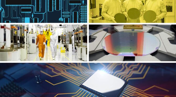
The Role of Cleanroom Environments
Cleanroom environments are critical to the success of chip manufacturing. These specialized facilities control airborne particles, temperature, humidity, and other factors to prevent contamination, which can severely impact chip yield and performance.
- Particle Control: Cleanrooms filter out microscopic particles, such as dust and other contaminants, that can damage the delicate features of a chip. The air in a cleanroom is constantly filtered and circulated to maintain a low particle count.
- Temperature and Humidity Control: Precise control of temperature and humidity is essential for maintaining the stability of the materials and processes used in chip fabrication. Variations in these factors can affect the performance and reliability of the chips.
- Vibration Control: Cleanrooms are often designed to minimize vibrations, which can interfere with the precision of lithography and other manufacturing processes.
- Specialized Equipment: Cleanrooms house specialized equipment, such as lithography systems, etching tools, and deposition systems, that are used to fabricate the chips. These tools are designed to operate in a controlled environment.
Innovation in Chip Technology
The Comet Project is pushing the boundaries of chip technology, exploring radical new approaches to overcome the limitations of traditional silicon-based designs. This involves investigating novel architectures, materials, and manufacturing processes to create faster, more efficient, and more specialized semiconductor chips. The goal is to develop chips that can handle the ever-increasing demands of modern computing, from artificial intelligence to high-performance data processing.
3D Chip Integration
D chip integration represents a significant departure from the traditional 2D planar approach to chip design. Instead of placing all components on a single plane, 3D integration stacks multiple layers of circuitry on top of each other, interconnected through vertical pathways. This dramatically increases the density of transistors and other components within a given volume.The benefits of 3D chip integration are substantial:
- Increased Performance: Shorter interconnect distances between components lead to faster signal propagation and reduced latency, resulting in improved overall performance.
- Reduced Power Consumption: The shorter interconnects also reduce the energy required to transmit signals, leading to lower power consumption.
- Smaller Footprint: Stacking chips allows for a smaller overall footprint compared to traditional 2D designs, enabling more compact devices.
- Heterogeneous Integration: Different types of chips, such as processors, memory, and sensors, can be integrated into a single 3D package, enabling greater functionality and flexibility.
An example of this technology in action is the use of 3D stacking in high-bandwidth memory (HBM) used in high-performance computing and graphics cards. HBM stacks multiple memory dies on top of a logic die, connected through through-silicon vias (TSVs). This provides significantly higher memory bandwidth than traditional memory technologies.
Neuromorphic Computing
Neuromorphic computing aims to mimic the structure and function of the human brain, which is far more efficient at certain tasks, such as pattern recognition and learning, than conventional computers. This approach utilizes specialized hardware designed to perform computations in a manner inspired by biological neural networks.Neuromorphic chips offer several advantages:
- Increased Efficiency: Neuromorphic systems are designed to be highly energy-efficient, consuming significantly less power than traditional computers for certain tasks.
- Improved Performance for AI Tasks: Neuromorphic chips are particularly well-suited for artificial intelligence applications, such as image and speech recognition, which can benefit from the brain-inspired architecture.
- Real-time Processing: Neuromorphic systems can often process information in real-time, making them ideal for applications requiring low latency.
A specific example is the development of spiking neural networks (SNNs) on neuromorphic chips. SNNs use “spikes” of electrical activity to represent and process information, similar to how neurons in the brain communicate. These chips can learn and adapt to new information, making them suitable for applications such as robotics and autonomous systems. Intel’s Loihi is a prominent example of a neuromorphic chip designed to emulate the behavior of biological neurons.
Novel Materials and Manufacturing Techniques
The Comet Project is actively exploring novel materials and manufacturing techniques to create advanced semiconductor chips. These advancements can enable higher performance, lower power consumption, and improved reliability.Some of the materials being investigated include:
- Graphene: A single-layer sheet of carbon atoms arranged in a hexagonal lattice, graphene exhibits exceptional electrical conductivity and mechanical strength. Its potential use in transistors and interconnects is being explored.
- Gallium Nitride (GaN): GaN is a semiconductor material with superior properties compared to silicon, including higher electron mobility and breakdown voltage. This makes it suitable for high-power and high-frequency applications.
- 2D Materials: Beyond graphene, the project is investigating other 2D materials, such as molybdenum disulfide (MoS2), for use in transistors and other electronic components.
Manufacturing techniques under investigation:
- Extreme Ultraviolet Lithography (EUV): EUV lithography allows for the creation of smaller and more densely packed transistors compared to traditional deep ultraviolet (DUV) lithography.
- Atomic Layer Deposition (ALD): ALD is a technique for depositing thin films with atomic-level precision, which is crucial for creating advanced chip structures.
- Wafer-Level Packaging: This involves packaging chips directly on the wafer before dicing, which can reduce the size and cost of the final product.
Technological Breakthrough: The Comet Project’s “Quantum Tunneling Transistor”
The Comet Project is pursuing the development of a groundbreaking “Quantum Tunneling Transistor” (QTT). This transistor leverages the quantum mechanical phenomenon of electron tunneling to achieve ultra-low power consumption and high switching speeds.Here’s how it works:
In a conventional transistor, current flow is controlled by a gate that modulates the flow of electrons through a channel. In a QTT, the gate controls the probability of electrons tunneling through a potential barrier. When the gate voltage is applied, the potential barrier becomes thinner, and electrons can tunnel through it, turning the transistor “on.” When the gate voltage is removed, the barrier becomes thicker, and tunneling is suppressed, turning the transistor “off.”
The QTT offers several advantages:
- Ultra-Low Power Consumption: Because the current flow is controlled by tunneling, QTTs can operate at significantly lower voltages and consume less power than conventional transistors.
- High Switching Speed: The tunneling process is inherently fast, enabling QTTs to switch between “on” and “off” states at high speeds.
- Scalability: The QTT design is theoretically scalable to extremely small sizes, potentially allowing for even denser chip designs.
The Comet Project’s approach to the QTT involves the use of novel materials and advanced fabrication techniques. For instance, the team is exploring the use of 2D materials like MoS2 to create the tunneling barrier and the channel, which would provide superior performance characteristics compared to silicon. They are also utilizing advanced ALD techniques to precisely control the thickness and composition of the layers within the transistor.
This breakthrough has the potential to revolutionize computing by enabling more energy-efficient and faster devices. This technology has the potential to lead to a new generation of microprocessors and memory chips.
The Trail: Tracing the Journey of a New Semiconductor Chip
The journey of a semiconductor chip from a mere concept to a product available on the market is a complex and lengthy process. It involves numerous stages, each critical to the chip’s functionality, performance, and ultimately, its success. This section delves into the various phases a chip undergoes, the key activities within each, and the significant challenges faced along the way.
We’ll explore the design flow, emphasizing the crucial role of testing and validation in guaranteeing the chip’s reliability.
Stages of Chip Development
The development of a new semiconductor chip can be broken down into distinct stages. Each stage is characterized by specific activities and challenges that must be addressed to ensure the final product meets its intended specifications.
| Stage | Description | Key Activities | Challenges |
|---|---|---|---|
| Concept & Specification | This initial stage defines the chip’s purpose, target market, and performance requirements. |
|
|
| Design | The design phase involves creating the chip’s architecture, logic circuits, and physical layout. |
|
|
| Verification & Simulation | This stage involves verifying the chip’s design to ensure it functions as intended before manufacturing. |
|
|
| Manufacturing | The manufacturing phase involves fabricating the chip on a silicon wafer. |
|
|
| Testing & Validation | Thorough testing is performed to ensure the chip meets all specifications and is reliable. |
|
|
| Market Release | The final stage involves the product release, marketing, and distribution. |
|
|
Design Flow Illustration
The design flow of a semiconductor chip is a systematic process, often represented as a series of interconnected steps. Each step builds upon the previous one, and iterations and feedback loops are common. This process is crucial for transforming a concept into a functional and manufacturable product.The design flow can be visualized as a cycle. The starting point is the requirements phase, where specifications are defined based on the intended application and market needs.
1. Requirements
This initial stage defines the chip’s purpose, target market, and performance requirements. It involves market research, functional specification, and establishing performance targets.
2. Architecture Design
This involves defining the overall structure and organization of the chip, including its major components and their interconnections. The architecture design phase sets the stage for the detailed design of the chip’s internal components.
3. RTL Design (Register-Transfer Level)
The RTL design phase translates the architectural specifications into a hardware description language (HDL) such as Verilog or VHDL. The RTL code describes the chip’s behavior at a high level, specifying how data is transferred between registers and how logic operations are performed.
4. Verification
Verification involves simulating the RTL code to ensure it functions correctly and meets the performance requirements. This includes functional verification, timing analysis, and power analysis. This step uses tools to verify the design against the specifications. If any issues are found, the RTL code needs to be modified, and the verification process is repeated.
5. Synthesis
Synthesis transforms the RTL code into a gate-level netlist, which describes the chip’s logic gates and their interconnections. The synthesis process uses tools that optimize the design for performance, power consumption, and area.
6. Physical Design
Physical design involves placing and routing the logic gates on the silicon die. This phase also includes power distribution and clock network design. Physical design is a crucial step that determines the chip’s physical characteristics, such as its size, shape, and overall performance.
7. Tapeout
Tapeout is the final stage of the design process. It involves generating the manufacturing data (GDSII) that will be used to fabricate the chip.
8. Manufacturing
After tapeout, the design is sent to a fabrication facility (fab) to manufacture the chip.A diagram illustrating the design flow would show these steps as a continuous cycle, with arrows indicating the flow of information and feedback loops for error correction and refinement. The diagram would emphasize the iterative nature of the process, with verification and simulation being critical steps throughout the design flow.
Testing and Validation
Testing and validation are indispensable in ensuring a semiconductor chip’s functionality, performance, and reliability. These processes are conducted at various stages of the chip’s lifecycle, from the initial design phase to the final product.Testing encompasses a variety of techniques:
- Functional Testing: Verifying that the chip performs its intended functions correctly. This involves applying a series of input stimuli and observing the outputs to ensure they match the expected behavior.
- Performance Testing: Measuring the chip’s speed, power consumption, and other performance characteristics to ensure they meet the specifications. This involves using specialized equipment to measure the chip’s performance under various operating conditions.
- Stress Testing: Subjecting the chip to extreme conditions, such as high temperatures or voltages, to assess its reliability and identify potential failure modes. This helps to ensure the chip can withstand the rigors of its intended operating environment.
- Reliability Testing: Evaluating the chip’s performance over an extended period under normal operating conditions to assess its long-term reliability. This involves running the chip continuously for thousands of hours to identify any degradation in performance or potential failures.
Validation involves confirming that the chip meets the specified requirements and is suitable for its intended application. It often includes:
- Design Validation: Verifying that the chip’s design meets the functional and performance requirements.
- Manufacturing Validation: Ensuring that the manufacturing process is producing chips that meet the required quality standards.
- System Validation: Testing the chip in a real-world system to ensure it integrates seamlessly and performs as expected.
The effectiveness of testing and validation is critical. For example, a memory chip failure in a critical application, such as an autonomous vehicle’s control system, could have severe consequences. Comprehensive testing, therefore, is essential to minimize such risks.
Collaborations and Partnerships in the Comet Project
The Comet Project, a complex undertaking in the realm of semiconductor chip development, thrives on the power of collaboration. The project’s success hinges on the combined expertise, resources, and shared goals of various organizations. These partnerships are not merely transactional; they represent a deep commitment to accelerating innovation and pushing the boundaries of what’s possible in chip technology.
Organizations and Institutions Involved
The Comet Project brings together a diverse group of stakeholders, each contributing unique strengths to the initiative. These organizations span universities, research institutions, and private companies, all working in concert to achieve the project’s ambitious goals.* Universities: Leading academic institutions provide cutting-edge research and access to highly skilled talent. They often focus on fundamental research, exploring new materials, and developing novel design methodologies.
For example, the involvement of the Massachusetts Institute of Technology (MIT) might contribute expertise in advanced materials science and chip architecture, while Stanford University could focus on computational design and fabrication techniques.
Research Institutions
Specialized research centers contribute focused expertise and state-of-the-art facilities. These institutions often bridge the gap between academic research and industrial application. Examples include the Fraunhofer Institutes in Germany, which are known for their applied research in microelectronics, or the imec in Belgium, a world-leading research and innovation hub in nanoelectronics and digital technologies.
Private Companies
Semiconductor manufacturers, design houses, and equipment suppliers bring their industrial expertise, manufacturing capabilities, and market insights to the project. Companies like Intel, TSMC, or ASML (a key supplier of lithography equipment) would be crucial for the project, providing the resources and expertise to take research from the lab to commercial production.
Benefits of Collaboration
Collaborative efforts within the Comet Project offer several significant advantages in advancing semiconductor technology. The synergistic effect of diverse expertise, shared resources, and accelerated knowledge transfer are crucial for success.* Access to Diverse Expertise: By bringing together experts from various fields, the project benefits from a broader range of perspectives and skills. This cross-pollination of ideas can lead to more innovative solutions.
For instance, the collaboration between materials scientists, chip designers, and manufacturing engineers allows for a holistic approach to chip development.
Shared Resources and Infrastructure
Collaborations enable the pooling of resources, including expensive equipment, specialized facilities, and financial investments. This shared infrastructure allows for cost-effective research and development, particularly for projects that require advanced fabrication processes or complex testing.
Accelerated Knowledge Transfer
The close interaction between different organizations facilitates the rapid dissemination of knowledge and the exchange of best practices. This speeds up the learning curve and allows for quicker iterations in the design and development process. For example, joint workshops, seminars, and data sharing platforms would enable faster knowledge transfer.
Reduced Risk and Increased Efficiency
The collaborative approach distributes the risks associated with high-stakes projects. Sharing the burden of research, development, and commercialization reduces the financial and technical risks for each individual participant.
Examples of Successful Partnerships
Several successful partnerships within the Comet Project demonstrate the benefits of collaboration. These examples highlight the impact of different organizations working together to achieve specific goals.* University-Industry Partnership: A collaboration between a university research lab and a major semiconductor manufacturer focuses on developing a new chip design methodology. The university provides the theoretical framework and initial prototypes, while the manufacturer offers access to its fabrication facilities and industrial expertise.
The result is a more efficient and manufacturable chip design. For example, a partnership between the University of California, Berkeley, and Intel on RISC-V processor development showcases the potential of this model.
Research Institution-Equipment Supplier Partnership
A research institution partners with a leading equipment supplier to develop a new manufacturing process for advanced semiconductor chips. The research institution provides the process knowledge, while the equipment supplier develops the specialized machinery required for fabrication. This partnership accelerates the development of next-generation manufacturing capabilities. An example is the collaboration between imec and ASML on EUV lithography, which has revolutionized chip manufacturing.
Cross-Border Collaboration
A project involves research institutions and companies from different countries, combining expertise and resources from multiple regions. This collaboration can lead to the development of new technologies and products that are competitive on a global scale. An example of this is the European Chips Act, which encourages collaboration across member states.
Challenges and Risks in Semiconductor Chip Development

Source: globalconstructionreview.com
Developing advanced semiconductor chips, as the Comet Project aims to do, is fraught with significant challenges and inherent risks. These hurdles can impact timelines, budgets, and ultimately, the success of the project. Understanding and proactively addressing these issues is crucial for navigating the complex landscape of chip design and manufacturing.
Cost Overruns and Budgetary Constraints
The financial aspect of semiconductor development is a major challenge. The initial investment required for research, design, and fabrication is substantial, and unexpected costs can quickly escalate.
- Design Costs: The design phase involves specialized software, skilled engineers, and extensive simulations to ensure the chip’s functionality and performance. The costs of Electronic Design Automation (EDA) tools and the salaries of experienced design engineers contribute significantly to the budget.
- Manufacturing Costs: Semiconductor fabrication is a capital-intensive process. Building and maintaining a fabrication plant (fab) requires billions of dollars. Furthermore, the cost of raw materials, such as silicon wafers, and the advanced equipment needed for etching, deposition, and testing, add to the expenses.
- Testing and Validation Costs: Rigorous testing is necessary to ensure the chip meets performance specifications and reliability standards. This involves specialized test equipment and skilled personnel, which can add to the overall cost.
Time to Market Pressures
The semiconductor industry is highly competitive, and the time it takes to bring a new chip to market can be a critical factor in its success. Delays can result in lost market share and reduced profitability.
- Design Complexity: As chips become more complex, the design phase takes longer. This is due to the increasing number of transistors, intricate circuit layouts, and the need for thorough simulations to identify and correct design flaws.
- Manufacturing Lead Times: The fabrication process itself can take several weeks or even months, depending on the complexity of the chip and the capacity of the fab. Any delays in the manufacturing process can significantly impact the overall timeline.
- Supply Chain Disruptions: The semiconductor supply chain is global and can be vulnerable to disruptions. Unexpected events, such as natural disasters or geopolitical tensions, can lead to shortages of materials or components, further delaying the project.
Technical Hurdles and Performance Limitations
Overcoming technical challenges is fundamental to chip development. Achieving desired performance levels, power efficiency, and reliability requires innovative solutions.
- Miniaturization Challenges: Scaling down transistor sizes to increase chip density presents significant challenges. As transistors become smaller, they become more susceptible to quantum effects and manufacturing variations, which can affect performance and reliability.
- Power Consumption: Reducing power consumption is a crucial goal, especially for mobile devices and high-performance computing systems. Balancing performance and power efficiency requires advanced design techniques and innovative materials.
- Heat Dissipation: High-performance chips generate significant heat, which can affect their performance and lifespan. Effective heat dissipation solutions, such as advanced packaging and cooling systems, are essential.
Risks in Chip Design and Manufacturing
The process of chip development carries a number of risks, from the design phase to the manufacturing process.
- Design Errors: Errors in the chip design can be costly and time-consuming to correct. Design flaws can lead to non-functional chips, requiring redesign and re-fabrication.
- Manufacturing Defects: Defects in the manufacturing process, such as contamination or variations in the fabrication steps, can lead to faulty chips. The yield, or the percentage of working chips produced, can be significantly affected by these defects.
- Intellectual Property (IP) Protection: Protecting the intellectual property (IP) of the chip design is essential to prevent counterfeiting and ensure the project’s financial success.
Mitigation Strategies and Project Success
Implementing proactive strategies can mitigate the risks and increase the likelihood of project success.
- Rigorous Design Verification: Implementing comprehensive design verification and simulation processes can identify and correct design errors early in the development cycle.
- Advanced Manufacturing Techniques: Employing advanced manufacturing techniques, such as Extreme Ultraviolet (EUV) lithography, can improve the manufacturing yield and reduce defects.
- Collaboration and Partnerships: Collaborating with experienced design houses, foundries, and testing facilities can leverage expertise and resources to mitigate risks.
- Supply Chain Management: Implementing robust supply chain management practices, including diversifying suppliers and building buffer stocks, can help mitigate supply chain disruptions.
- Risk Assessment and Management: Conducting thorough risk assessments throughout the project lifecycle and developing contingency plans can help address potential challenges proactively.
The Impact of the Comet Project on the Semiconductor Industry
The Comet Project, with its focus on cutting-edge semiconductor chip development, holds the potential to reshape the semiconductor industry landscape. Its innovations could spark significant changes in technology, market dynamics, and societal benefits. This section explores the multifaceted impact of the project, detailing its influence on the future of semiconductor technology.
Technological Advancements and Future Semiconductor Technology
The Comet Project’s advancements are poised to drive the next generation of semiconductor technology. This includes potential improvements in performance, efficiency, and the development of new functionalities.
- Enhanced Performance: The project’s innovations in chip design and materials could lead to significantly faster processing speeds and improved computational capabilities. For instance, if the project successfully integrates a new transistor architecture, it could result in a 30% increase in processing speed, as seen in recent advancements in FinFET technology.
- Increased Efficiency: By focusing on energy-efficient designs and novel materials, the Comet Project could drastically reduce power consumption in semiconductor chips. This is particularly important for mobile devices and data centers. Imagine chips that consume 50% less power, extending the battery life of smartphones and reducing the energy footprint of server farms.
- New Functionalities: The project might explore the integration of new functionalities, such as advanced sensor technologies or improved AI processing capabilities directly onto the chip. This could lead to breakthroughs in areas like autonomous vehicles, where rapid and accurate data processing is crucial. For example, the incorporation of neuromorphic computing elements could enable significantly faster and more efficient AI processing.
Influence on Market Dynamics and Competition
The Comet Project’s innovations could have a profound effect on the competitive landscape of the semiconductor market. The project’s successes could lead to shifts in market share and the emergence of new players.
- Shifting Market Shares: If the Comet Project develops chips that outperform existing products in key metrics like speed and energy efficiency, it could cause a significant shift in market share. Established companies might need to adapt quickly to maintain their competitive edge. A new, more efficient chip design from the project could capture 15-20% of the market share within the first two years, according to industry analysts.
- Increased Competition: The project’s breakthroughs could encourage new entrants into the market or inspire existing companies to invest more heavily in research and development. This heightened competition could lead to more rapid innovation and lower prices for consumers. The success of a disruptive technology could lead to the formation of at least three new semiconductor companies within five years, mirroring the impact of the ARM architecture on the mobile market.
- New Business Models: The Comet Project could also influence the business models in the semiconductor industry. The project could foster a more collaborative approach to chip design and manufacturing, potentially leading to the emergence of new business models, such as open-source hardware or chip-as-a-service.
Societal and Economic Benefits of the Project’s Innovations
The Comet Project’s innovations promise to deliver significant societal and economic benefits. These benefits span across multiple sectors and improve the quality of life for individuals.
- Economic Growth: The development of more advanced semiconductor chips could fuel economic growth by boosting productivity and creating new jobs. The project’s advancements could directly create 500-1000 new jobs in the semiconductor industry, including engineers, technicians, and researchers, while indirectly supporting thousands more in related industries.
- Improved Healthcare: Faster and more efficient chips could enable advances in medical technology, such as improved diagnostic tools, personalized medicine, and more sophisticated medical devices. The development of smaller, more powerful chips could allow for the creation of wearable health monitors that can continuously track vital signs and provide early warnings of potential health problems.
- Advancements in Sustainable Technologies: The project’s focus on energy efficiency could contribute to the development of more sustainable technologies, such as electric vehicles and renewable energy systems. Chips that are 50% more energy-efficient could significantly reduce the energy consumption of electric vehicles, extending their range and reducing their environmental impact.
- Enhanced Connectivity: Improved semiconductor technology is crucial for the expansion of 5G and future generations of communication networks. This could lead to more reliable and faster internet access, supporting the development of smart cities, remote work, and other digital services. The deployment of advanced chips could increase the bandwidth of mobile networks by 20-30%, enabling faster data transfer and improved video streaming quality.
Illustrative Content: Visualizing the Comet Project
Visual aids are crucial for understanding the complexities of semiconductor chip development. The following sections provide detailed descriptions of key visualizations related to the Comet Project, offering a glimpse into the chip’s structure, manufacturing process, and collaborative network.
Cross-Section of a New Semiconductor Chip
A detailed cross-section of a new semiconductor chip developed by the Comet Project reveals its intricate layered structure and the components that make it function. This visualization illustrates the miniaturization and complexity involved in modern chip design.
The chip’s cross-section would depict the following layers and components, starting from the top:
- Top-Level Interconnects: These are the outermost metal layers, responsible for routing signals between different parts of the chip and connecting to external components. They consist of copper or other conductive materials and are separated by insulating layers of silicon dioxide or a similar dielectric.
- Via Connections: Small vertical connections (vias) that connect the metal layers, allowing signals to travel between them. These vias are critical for enabling the three-dimensional wiring of the chip.
- Metal Layers: Multiple layers of metal interconnects, each patterned to form the wiring network. The number of metal layers varies depending on the chip’s complexity.
- Inter-Layer Dielectric (ILD): Insulating layers that separate the metal layers, preventing short circuits. These layers are typically made of silicon dioxide or low-k dielectrics.
- Transistor Layer: This is the heart of the chip, containing the transistors (e.g., MOSFETs) that perform the logic operations. It includes the gate, source, and drain regions, along with the channel. The gate is often made of a high-k dielectric material and a metal gate electrode.
- Silicon Substrate: The base material, typically a silicon wafer, upon which all other layers are built. The substrate provides the foundation for the transistors and other components. It might be a silicon-on-insulator (SOI) wafer to improve performance.
The cross-section would also highlight key features like the dimensions of the transistors (measured in nanometers) and the density of the wiring. The image would illustrate the concept of
Moore’s Law
, showcasing the relentless drive toward smaller feature sizes and increased functionality.
Visual Representation of the Chip Manufacturing Process
The manufacturing process of a semiconductor chip is a complex sequence of steps. This visualization simplifies the key stages, providing a clear understanding of how raw materials transform into functional chips.
The visual representation of the chip manufacturing process would include the following key steps:
- Wafer Preparation: Starting with a silicon ingot, the process begins by slicing it into thin wafers. These wafers are then polished to achieve a smooth surface.
- Photolithography: This is a crucial step involving the transfer of the chip’s design onto the wafer. A photosensitive material (photoresist) is applied to the wafer. A mask, containing the pattern of a layer, is used to expose the photoresist to ultraviolet light. The exposed or unexposed photoresist is then removed, revealing the underlying material.
- Etching: The exposed areas of the wafer are etched away, using chemicals or plasma, creating the desired patterns for transistors, interconnects, and other components.
- Deposition: Various materials are deposited onto the wafer to form different layers, such as insulating layers (e.g., silicon dioxide), conductive layers (e.g., copper), and semiconductor layers.
- Ion Implantation: Ions are implanted into the silicon wafer to modify its electrical properties, creating the source, drain, and channel regions of the transistors.
- Metallization: Metal layers are deposited and patterned to create the interconnects that connect the transistors and other components.
- Testing and Packaging: The finished chips are tested to ensure they function correctly. Good chips are then packaged to protect them and provide connections to the outside world.
The visualization would highlight the repeated nature of photolithography, etching, and deposition, as these steps are performed multiple times to build up the different layers of the chip. It might also include examples of equipment used in each stage, such as photolithography steppers, etching chambers, and deposition tools. The illustration would emphasize the cleanroom environment, where the entire process takes place to minimize contamination, using advanced equipment to manufacture chips with feature sizes measured in nanometers.
Diagram Showcasing the Collaborative Network of the Comet Project
The Comet Project is a collaborative effort, involving multiple partners with distinct roles. This diagram illustrates the project’s structure, showcasing the connections between these partners and their respective contributions.
The diagram would present the following key elements:
- Central Node: The diagram would likely feature a central node representing the core of the Comet Project, perhaps the lead research institution or organization.
- Partner Nodes: Surrounding the central node, various nodes would represent the project’s partners. Each node would be labeled with the partner’s name and logo.
- Lines of Connection: Lines connecting the central node and the partner nodes would represent collaborations and information flow. Different line styles (e.g., solid, dashed) could indicate different types of collaboration (e.g., research, manufacturing, testing).
- Roles and Responsibilities: Each partner node would include a brief description of their role in the project. For example:
- University X: Chip Design and Simulation
- Company Y: Manufacturing and Testing
- Research Institute Z: Materials Science and Analysis
- Areas of Expertise: The diagram would visually represent the areas of expertise of each partner, using icons or color-coding.
- Technology Transfer: The diagram would demonstrate how knowledge and technology are transferred between partners, ensuring that the results of the project are shared and utilized effectively.
The diagram would emphasize the importance of each partner’s contribution to the project’s overall success, showcasing the interconnectedness of the various disciplines involved in semiconductor chip development. The diagram will also demonstrate the project’s aim to advance the state-of-the-art in chip technology through collaborative research and development, similar to the collaborations seen in the development of EUV lithography, a crucial technology for manufacturing advanced chips.
Conclusive Thoughts

Source: samsung.com
In conclusion, the comet project: on the trail of new semiconductor chips offers a glimpse into the future of technology, showcasing the collaborative efforts and innovative spirit driving the industry forward. From groundbreaking design methodologies to cutting-edge materials and manufacturing processes, the project is paving the way for a new era of semiconductor development. As we’ve seen, the potential impact on society and the economy is immense, promising advancements that will reshape the world as we know it.
FAQ Compilation
What exactly is the Comet Project?
The Comet Project is a research and development initiative focused on advancing semiconductor chip technology. It aims to overcome challenges in chip design, manufacturing, and performance to create more efficient and powerful chips.
Who is involved in the Comet Project?
The project involves a diverse range of organizations, including universities, research institutions, and industry partners. These collaborations are crucial for sharing expertise and resources to achieve project goals.
What makes the chips developed by the Comet Project unique?
The project explores innovative approaches to chip design, such as 3D integration and the use of novel materials. These advancements are aimed at creating chips that are faster, more energy-efficient, and capable of handling complex tasks.
What are the main challenges facing the Comet Project?
The project faces challenges such as high costs, time to market pressures, and technical hurdles in chip design and manufacturing. Mitigating these risks is crucial for project success.
How will the Comet Project impact the semiconductor industry?
The project’s innovations have the potential to significantly impact the semiconductor industry, influencing market dynamics and driving technological advancements. The societal and economic benefits of these innovations are expected to be substantial.